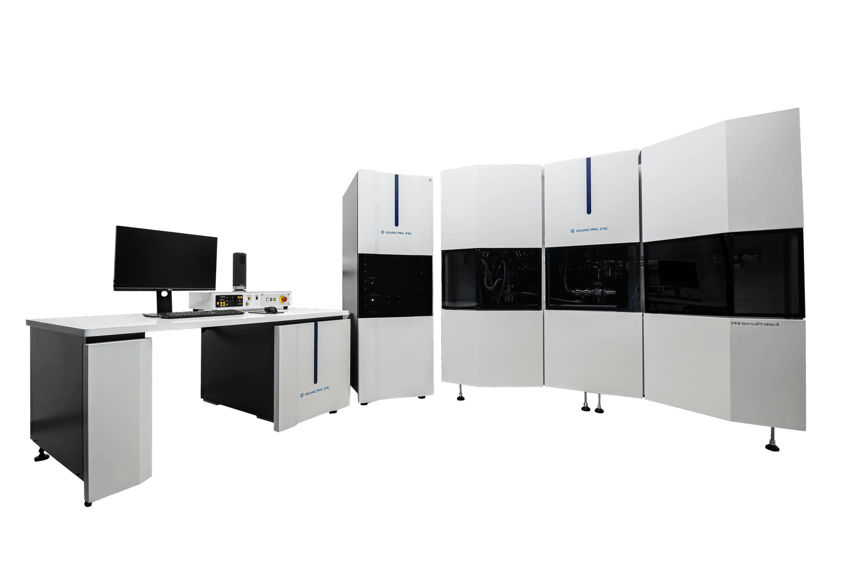
Multi-Technique Surface Analysis System(XPS, AES, UPS, LEIPS)
Asset number
MC-SA-0002
Model
PHI VersaProbe4
Brand
ULVAC-PHI
Asset Leader
侯雨箫 Yuxiao HOU
Contact email
Location
W2-142
Main specifications
1. Monochromatic X-ray source system (electron gun, anode target and monochromator)
2. Energy Analyzer: Energy resolution on Ag: ≤ 0.48 eV at Ag3d5/2 (FWHM)
3. Argon Ion Gun Energy: 0 - 5 kV; GCIB argon cluster ion gun maximum energy: 20 kV
4. Energy resolution of Dual-Beam Charge Neutralization System for PET: count rate of C-C peaks in C1s spectra ≥ 60,000 cps, FWHM of O-C=O peaks ≤ 0.85 eV
5. LEIPS (Ultraviolet Photoelectron Spectroscopy System): Fermi fringe width <100 meV at room temperature (20% and 80%)
6. LEIPS (Low Energy Inverse Photoelectron Spectroscopy System) energy resolution: filter: 254 nm + 300 nm (LP) (4.88 eV) - Fermi edge width < 0.45 meV at room temperature (20% and 80%)
7. SAM scanning OSCE system (also provides REELS analysis capability)Maximum energy: 10 kV, spatial resolution: ≤100 nm
Main functions
1. Continuously adjustable X-ray focus beam spot is from less than 10µm to 400µm, by scanning the analysis area up to 1.4mm X 1.4mm, meeting the needs of analysis from micro-area (less than 7.5µm) to millimeter scale.
2. SXI imaging, suitable for analysis of film layer structure of solid-state battery materials, interfacial composition distribution, differential analysis of different micro-zone compositions, etc. Per image only takes 1-5s.
3. Dual-Beam Charge Neutralization/Compensation System that uses cold cathode electron flow and very low energy ions from an argon ion sputtering gun to charge neutralize all types of samples.
4. 20 kV Ar GCIB for deep profiling of cell materials
5. Variable angle XPS analysis, only for self-assembled film systems with very thin surface layers (1-5 nm). The longitudinal distribution of the composition from the surface to several nanometers’ depth is obtained by changing the receiving angle of the photoelectrons (tilting the sample stage) and changing the receiving depth of the photoelectrons.
6. In-situ XPS-UPS-IPES: XPS (surface composition), UPS (valence band spectrum and power function), IPES (conductivity spectrum) can be tested under the same vacuum conditions (analysis chamber). Excellent for semiconductor materials, organic photovoltaics, OLED, photocatalysis, etc.
Precautions for sample testing
样品要求:样品尺寸长宽介于1~1.5cm之间,厚度小于0.5cm的薄片状样品。样品必须适用于真空环境,应当为固体或粉末,不含有毒、有害、挥发性、有腐蚀性及放射性物质,磁性样品送样前需要提前咨询。
主要附件:
1. X 射线光电子能谱(XPS)
2. 俄歇电子能谱(AES)
3. 低能反向光发射光谱学(LEIPS)
4. 反射电子能量损失光谱学(REELS)
5. GCIB/Ar源,可以提供深度剖析分析